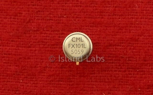
FX101L Frequency Switch
Frequency Sensitive Switch
Features
- DATUM OR BAND SWITCHING
- ADJUSTABLE SWITCH FREQUENCIES
- HIGH STABILITY SET POINTS
- NARROW BAND/WIDE BAND SWITCHING
- SINE 0R PULSE SIGNAL INPUT
- SWITCH LATCHING OPTIONS
Description
The FX-101L is a high-performance frequency sensitive switch constructed in a monolithic form using MOS/MSI techniques. It is a pin and function compatible equivalent of the standard CML FX-101, but offers improved accuracy and operates from lower supplies voltage. The FX-101 L is the preferred version for new equipment and systems in the course of planning, and in many cases can be employed as a direct plug-in replacement for the FX-101 in existing applications.
The FX-101L accepts sine wave or pulse input signals and operates an integral semiconductor switch when the input frequency reaches an accurately predetermined value. By just grounding or floating a control input pin the FX-101L may be arranged to switch 'ON' when the input frequency lies anywhere above a single datum value (Datum Model or within a preset band of values (Band-Mode). The switch set points may be varied over a wide range of frequencies according to the values of two external resistors and two capacitors. Setpoint stability is of a high order and is maintained over the entire specified range of supply voltages and operating temperatures. Setpoint thresholds are extremely sharp and yield an effective Q factor exceeding 1000; the FX-101L also exhibits a fast response time combined with exceptional immunity to turn-on by random signal noise.
In addition to the Datum/Band functions, the FX-101L has control inputs which allow a choice of Latch or Unlatched switch operation, which includes Latch to on or Latch to off in the latch mode. Further facilities include, direct switch reset, and selection of Fail Safe (switch OFF), delayed Fail Safe or Ignore (hold state) switching options in the event of the signal interruption. Function control inputs are high impedance and may be operated by external logic levels.
The FX-101L is housed in a ten lead TO-100 style package and operates from a single wide tolerance DC supply of -8V to -15V, over the extended temperature range.
Operating Principle
The tone recognition system employed by the FX-101L is based on a period sampling technique. Input signals are amplified and shaped to provide clock signals to the bistable flip-flop, the output of which is a square wave having a period equal to the interval between successive input waveform zero-crossings.
The flip-flop output triggers a monostable (M1) which generates a reference period corresponding to 1/f1, where f1 (Hz) represents the Datum mode set-point, or the upper edge of the Band mode tone accept channel. At the expiry of the M1 period, monostable M2 is triggered; the summed periods M1 + M2 corresponding to 1/f2, the lower edge of the tone accept channel.
The reference periods are compared against the signal input period in a comparator, the output of which controls a special counter/storage system. This counting system discriminates against random spurious information and delivers an output only when many sampled periods have a true average value falling within the 'tone accept' limits. The output of the counter system, which is continuously monitoring the input information, is applied to the output buffer switches. Gating circuits are incorporated which prevent false operation when harmonics of the tone frequency are applied.
This unique and patented tone recognition system yields extremely sharp tone channel definition, coupled with a fast response time and high immunity to false turn-on due to out-band noise, regardless of the noise frequency and amplitude. The period sampling system requires, however, a regular input waveform for correct operation. Input noise can, if mixed with the required inband tone, prevent the circuit from recognising that the tone is present, This effect is produced because the noise jitters the interval between successive signal zero crossings and the comparator/counter rejects the information as not being consistent with an input signal having a frequency actively within the tone channel limits.
If the noise is random in nature, e.g. spurious noise spikes or short term interference (short in relation to the device recognition time or inband tone duration) it has little or no effect other than possibly to increase the overall tone recognition time by a few cycles. If the noise is continuous, e.g. parallel inband and out band tones are on the signal line simultaneously, the device does not recognise the inband tone. If the noise is semi-continuous, e.g. speech signals, increasing the inband tone duration will allow the tone to be recognised during a momentary 'noise' pause.
The device is, therefore, ideal for use when inband tones are transmitted individually, or sequentially, but operation in parallel-tone signalling schemes is not recommended unless adequate pre-filtering is used.
General Circuit Operation
The tone recognition system employed by the FX-101L is based on a period sampling technique. Input signals are amplified and shaped to provide clock signals to the bistable flip-flop, the output of which is a square wave having a period equal to the interval between successive input waveform zero-crossings.
The flip-flop output triggers a monostable (M1) which generates a reference period corresponding to 1/f1, where f1 (Hz) represents the Datum mode set-point, or the upper edge of the Band mode tone accept channel. At the expiry of the M1 period, monostable M2 is triggered; the summed periods M1 + M2 corresponding to 1/f2, the lower edge of the tone accept channel.
The reference periods are compared to the signal input period in a comparator, the output of which controls a particular counter/storage system. This counting system discriminates against random spurious information and delivers an output only when many sampled periods have a true average value falling within the 'tone accept' limits. The output of the counter system, which is continuously monitoring the input information, is applied to the output buffer switches. Gating circuits are incorporated which prevent false operation when harmonics of the tone frequency are applied.
This unique and patented tone recognition system yields extremely sharp tone channel definition, coupled with a fast response time and high immunity to false turn-on due to out-band noise, regardless of the noise frequency and amplitude. The period sampling system requires, however, a regular input waveform for correct operation. Input noise can, if mixed with the required inband tone, prevent the circuit from recognising that the tone is present, This effect is produced because the noise jitters the interval between successive signal zero crossings and the comparator/counter rejects the information as not being consistent with an input signal having a frequency actively within the tone channel limits.
If the noise is random in nature, e.g. spurious noise spikes or short term interference (short compared to the device recognition time or inband tone duration) it has little or no effect other than possibly to increase the overall tone recognition time by a few cycles. If the noise is continuous, e.g. parallel inband and out band tones are on the signal line simultaneously, the device does not recognise the inband tone. If the noise is semi-continuous, e.g. speech signals, increasing the inband tone duration will allow the tone to be recognised during a momentary 'noise' pause.
The device is, therefore, ideal for use when inband tones are transmitted individually, or sequentially, but operation in parallel-tone signalling schemes is not recommended unless adequate pre-filtering is used.
Supply Notes
References to ground, logic 0 and logic 1 in this datasheet are based on the use of a grounded positive supply, i.e. VDD is negative. A logic 1 level is therefore near VDD (-VE) and a logic 0 level near ground (+VE). There is, however, no objection to operation with the -VE supply grounded, but the reference to logic polarities remain unchanged, i.e. a logic 1 is always -VE referenced to a logic 0.
Note also that the case is internally connected to the +VE pin and will, therefore, be above ground potential if VDD = 0V. It is also important to ensure that no pin receives a potential which is positive respect to the +VE supply pin. Failure to observe this rule may result in damage to the device.