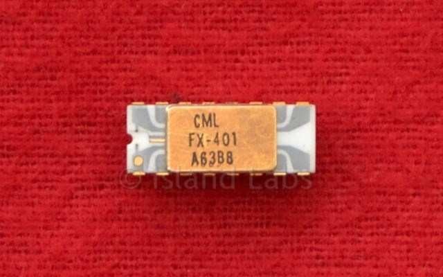
FX401 Frequency Switch
FX401 Frequency Sensitive Switch
Characteristics
Supply Voltage -12 V
Supply Current 3 mA
Input Range 0.1 - 15VPP
Set-Point Frequencies 1Hz - 20kHz
Switch 'ON' Resistance 1kΩ
Response Time 3ms
Set-Point Stability 0.05%
Set-Point Definition 0.1%
The FX-301L and FX-401 are two monolithic microcircuits which function as precision frequency sensitive switches. The FX-301 L is a single set-point switch intended for HI/LO switching operations, the FX-401 is a dual set-point version designed for sophisticated HI/IN-LIMIT/LO frequency monitoring systems.
Both devices are purpose-designed for 'analogue' frequency monitoring applications, such as Tachometry, Flow-rate and Process Control, where switching operations must be performed when a signal frequency reaches pre-determined levels.
These LSI (Large Scale Integration) circuits incorporate all the necessary signal amplifiers, reference generators, logic arrays and output switch drivers forming a fully operational sub-system. The only external components required are a few conventional resistors and capacitors, these allow the user to programme the switch operating frequencies, hysteresis and signal cut-off failsafe delay.
The FX-301L and FX-401 may be used individually, or in combination, to perform almost any required frequency operated switching function, from simple 'No Flow' alarms to complex multi-level precision monitors for high technology control systems. They are the most advanced state-of-art devices for this purpose available today and set new standards of economy and performance in this critical application area.
As an added assistance, two special printed circuit cards are also available. These are supplied ready drilled for the appropriate device and its external components, and allows experimental or prototype circuit arrangements to be rapidly and correctly set up by the engineer.
General Description
The frequency recognition system employed by the FX-301L and FX-401 is based on a period sampling technique. Input signals are amplified and shaped to provide clock signals to the bistable flip-flop, the output of which is a square wave, having a period equal to the interval between successive input waveform 'zero-crossings'.
The flip-flop output triggers a dual monostable, which generates reference periods corresponding to set-point f1 and set-point f2. These periods are determined by R1/C1 and R2/C2.
The reference periods are compared against the signal input period in one comparator (FX-301L) or two comparators (FX-401), the output/s of which control a particular counter/storage system. This counting system discriminates against random/spurious noise information and delivers an output only when a true input set-point frequency is received. Gating circuits are incorporated which prevent false operation when harmonics of the set-point frequencies are applied.
This frequency discrimination system yields an extremely sharp set-point definition coupled with fast response time and a positive 'chatter-free' switch-action.
As the device monitors all input signals applied, care should be taken to ensure that the input does not include noise signals having a frequency lying above the switch set-point levels.
For example, a magnetic pick-off may generate signals arising from vibration effects in addition to the right signal caused by passing gear teeth; if the frequency and amplitude of the vibration signals are high enough, they may operate the output switch. Short term spurious noise signals, for example, random spikes induced by contactor operation, will have little effect but may cause the switch response time to be increased if they occur as the input frequency reaches a set-point threshold.
FX-401 Operation
Fig. 3 illustrates the switching functions of the FX-401 Dual Datum Switch, for a continually varying signal input (as derived from the pick-up in a tachometry application). With no signal or a signal below f2, the decoding systems incorporated in the device, turn on the "Signal LO" output switch (pin 13). When the signal input reaches set-point f2, the internal counters trigger the decoding system, and the signal is recognised as an in-band frequency, turning ON the 'Signal in-band' switch (pin 11) and simultaneously switching OFF the 'Signal LO' switch. As the input signal progresses through set-point f1, the decoding system turns ON the 'Signal HI' switch (pin 9), simultaneously turning OFF the 'Signal inband' switch. The three switches are mutually exclusive, and only one switch is ON at any one time.
The mode control inputs (pins 14 & 15) allow various latching functions to be performed. These two input pins are logically controlled by either grounding (logic '0') or open-circuiting (logic '1’) the pin. With both control pins at '0,' the output switches are 'UNLATCHED' and operate
at the appropriate set-point frequencies, thus reflecting the present value of the signal input frequency. With both control pins at '1', 'LATCH OUT-BAND' mode, the HI or LO output switch will latch if the input signal deviates outside the INBAND zone, i.e. above f1 or below f2. 'LATCH HI' mode is obtained by applying '1' to pin 14 and '0' to pin 15, this latches the Output HI switch when the signal input lies above f1. LATCH LO mode requires '0' on pin 14 and '1' on pin 15, thus latching the signal L0 switch when the signal lies below f2. See fig.4 for latching Truth-Tables.
Once latched, a switch remains in the ON condition regardless of further input signal changes; to unlatch, or reset an output switch, the signal input must be returned to a non-latch value and a momentary '0' applied to both control pins.
A 'Signal Failure' recognition facility is incorporated in the circuit which allows a choice of switch actions if the input signals are cut-off instantaneously (see section on Signal Failure).
A further useful facility is the Output Inversion option provided by Pin 16. By applying '0' or '1' level to this pin, the of all three output switches are reversed. This allows the user the choice of energising or de-energising an external switch load when the set-point frequency is reached.
Each control input (pins 14, 15 and 16) is provided with an internal pull-up resistor which automatically places a '1' level (-ve) on the pin when the pin is open-circuit.
NOTE:
Set-point f1 should always be at a higher frequency than set-point f2. If component values are used which place f2 higher than f1, the INBAND zone disappears, and the output switches change directly from LO to HI at the frequency determined by the components used for set-point f1.