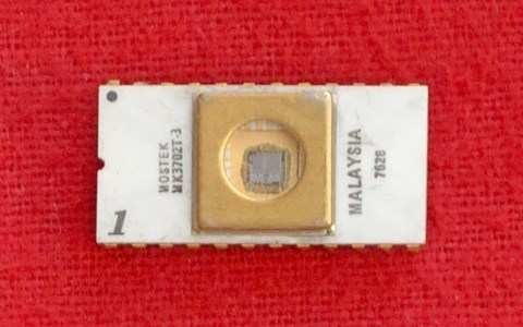
MK3702 EPROM
Features
- Replacement for the popular 1702A PROM
- Improved performance:
- Random access of 550ns (-1)
- 750ns (-2)
- 1µs (-3)
- No VGG power supply required
- All inputs TTL compatible
- Three-state TTL-compatible outputs -"OR-tie" capability
- High speed programming: Typically 30 seconds for all 2048 bits using standard PROM (1702A) programmers with no modifications
- Hermetically sealed package with transparent lid
- Typical Application - Microprocessor system prototyping aid
Description
The MK 3702 is a 256 x 8-bit electrically programmable and ultraviolet erasable Read Only Memory circuit, fabricated with MOSTEK's P-Channel Silicon-Gate technology. The MK 3702 PROM is ideally suited for applications where fast turnaround and pattern experimentation are important. The MK 3702 is a very reliable device that offers significant advantages over hard-wired logic in cost, system flexibility and performance. MOSTEK performs complete programming and functional testing on all 2048 bit locations prior to shipment to insure 100% programmability.
The MK 3702 is packaged in a 24-pin dual-in-line (DIP) package with a transparent, hermetically sealed lid. This allows the user to expose the chip to ultraviolet light to erase the bit pattern. A new pattern can be written into the device by following the programming procedures outlined in this data sheet. This procedure can be repeated as many times as required.
MOSTEK also has available the MK 3602 which is identical to the MK 3702 in every respect except for the package. The MK 3602 is packaged in a 24-pin DIP with a metal lid. Therefore, the MK 3602 is not erasable by exposure to ultraviolet light.
Programming Instructions
1. Operation in the Program Mode
(MK 3602/MK 3702)
Initially, all 2048 bits of the ROM are in the "0" state (output low). Information is introduced by selectively programming "1s" (output high) in the proper bit locations. Word address selection is done by the same decoding circuitry used in the READ mode (see logic levels). The address should be programmed in the sequence 0 through 255 for a minimum of 32 times. The eight output terminals are used as data inputs to determine the information pattern in the eight bits of each word. A low data input level (-48V) will program a "1" and a high data input level (ground) will leave a "0". All eight bits of one word are programmed simultaneously by setting the desired bit information patterns on the data input terminals. During the programming procedure, VDD and the Program Pulse are pulsed signals.
2. MK 3702 Erasing Procedure
The MK 3702 may be erased by exposure to high intensity ultraviolet light by illuminating the chip through the window. This exposure to ultraviolet light induces the flow of a photo current from the floating gate. to .the substrate, thereby discharging the gate to its initial state. An ultraviolet light source of 2537 A yielding a total integrated dosage of 6W-sec/cm2 is required. Note that the MK 3702 will be completely erased, as there is no known method of selectively erasing any portion of the chip.
The lamps should be used without short-wave filters, and the MK 3702 to be erased should be placed about one inch away from the lamp tubes.
