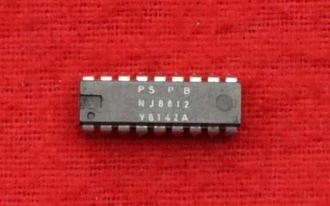
NJ8812 Synthesiser
Features
- High-Frequency Range
- Low Pin Count
- Direct interface to ROM or PROMS
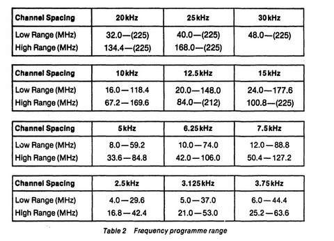
- Preset Channel Spacings 20, 25, 30 kHz and Sub Multiples
- High Comparison Frequency
- Low-Level Sinewave Crystal Oscillator Input up to 10 MHz
- Systems Clock Available — Constant Data Select Frequency of 1.2kHz (Reference Oscillator = 4.8MHz)
- Microprocessor Compatible
Description
The NJ8812 is an N-channel MOS integrated circuit that provides all the decoding and controlling circuitry for frequency synthesisers. It is intended to be used in conjunction with a 2-modulus prescaler such as the SP8793 to produce a universal binary coded synthesiser for mobile radio applications.
The NJ8812 can be described by 3 system blocks: the reference divider, the programmable divider, and the phase/frequency comparator, as shown in Fig.2. All control inputs and outputs are TTL compatible.
The Reference Divider
The reference divider is driven externally from a 4.8MHz crystal oscillator and can be externally preset to one of sixteen division ratios. These division ratios enable all commonly used reference frequencies to be applied to the phase/frequency comparator. Selection is accomplished using the two pins FA and FE. These pins may be connected to ground (logic ‘0') or left open circuit (logic '1'), connected to Data Select 1 output or to Data Select 2 output. On-chip decoding enables the latter two states to be recognised as independent states. All sixteen selections may be latched on-chip by grounding the Data Select 2 output. Table 1 gives reference frequencies that can be preset using a 4.8MHz crystal oscillator.
The data-select outputs (crystal oscillator frequency ÷ 4096) are independent of the preset reference frequency.
Programmable Divider
The programmable division section of the NJ8812 consists of a 6-bit programmable divider and an 8-bit programmable divider. The 6-bit divider controls the modulus of the external prescaler, and the 8-bit counter determines the total count period. The SP8793/NJ8812 combination is capable of dividing by all integer values between 1600 and 11839. When the Range pin on the NJ8812 is grounded, the programme range is shifted to between 6720 and 16959.
The programming data is multiplexed as 3 words of 4 bits and 1 of 2 bits completing a 14-bit binary number. This input data may be stored on-chip by grounding the Data Select 2 output after data transfer has occurred (See Fig.4).
All on-chip multiplexing may then be inhibited, if desired, by grounding Data Select 1 output.
Data Selection
To programme the synthesiser, the following information is required:
- The reference comparison frequency—typically equal to the channel spacing.
- The frequency of the VCO.
The frequency programme information is presented to the device in multiplexed form. The reading of this data by the device is controlled by the two data select outputs from the device. This sequence is shown in Fig.4.
Application Notes
The NJ8812 is designed for use in phase locked loop frequency synthesisers. In these synthesisers, the voltage controlled oscillator (VCO) operates at the output frequency, and the output frequency is divided down to a reference frequency. Another signal at this reference frequency is derived from the crystal controlled reference oscillator, and the divided VCO signal is compared at this frequency with the reference signal in a phase and frequency comparator. The output signal derived from this comparison consists of short pulses whose mark-space ratio is such that when the pulses are integrated, a DC level
is obtained, which, when applied to the VCO, locks the loop by maintaining the VCO on frequency.
Simple division to the reference frequency in a fully programmable divider is limited to frequencies of about 50 MHz and below, because of the difficulty of producing fully programmable dividers. However, a two-modulus divider which divides by N and N+1 may be easily made. A system as shown in Fig.5 then provides for the programmable division to be done at lower frequencies.
When out of lock, (ϕD and ϕU) have no definite phase relationship. These outputs may be combined in a suitable circuit, as shown in Fig.7.

