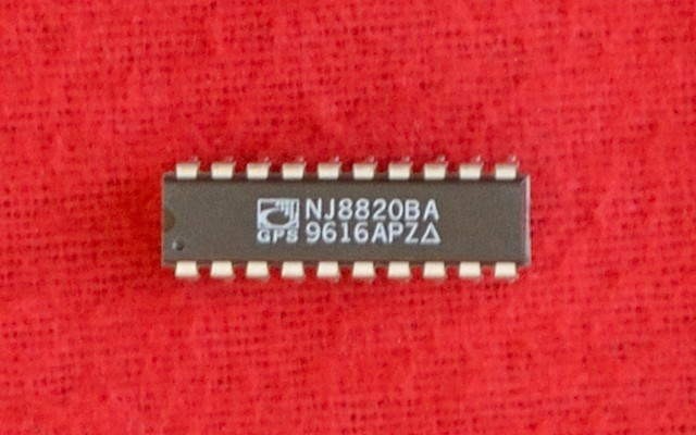
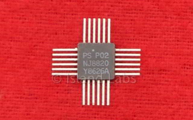
NJ8820 Synthesiser
Frequency Synthesiser (PROM Interface)
Features
- Direct Interface to ROM or PROM
- >10MHz Input Frequency
- Low Power Consumption
- High-Performance Sample and Hold Phase Detector
- Temperature range = -30°C to +70°C (NJ8820DP & MP)
- Temperature range = -40°C to +85°C (NJ8820B)
- Supply voltage = 5V ±0.5V
- Storage temperature -65°C to +150°C
The NJ8820/NJ8820B is a synthesiser circuit fabricated on the Plessey 5-micron CMOS process and is capable of achieving high sideband attenuation and low noise performance. The circuit contains a reference oscillator, 11-bit programmable reference divider, digital and sample-and-hold phase comparators, 10-bit programmable 'M' counter, 7-bit programmable 'A' counter and the necessary control and latch circuitry for accepting and latching the input data.
Data are presented as eight 4-bit words read from an external memory with the necessary timing signals generated internally. It is intended to be used in conjunction with a two-modulus prescaler such as the SP8710 series to produce a universal binary coded synthesiser.
The NJ8820 is available in Plastic DIL (DP) and Miniature Plastic DIL (MP) packages, both with an operating temperature range of -30°C to +70°C. The NJ8820B is available only in Ceramic DIL package with operating temperature range of -40°C to +85°C.
Programming
Twenty-eight data bits are required per channel arranged as eight 4-bit words leaving four redundant bits, two of which are available on the data bus driving the data-transfer time slot and may be used for external control purposes. A suitable PROM may be the 74S287 giving up to 32 channel capability as shown in Fig.5. Note that the choice of PNP transistor and supply bypass capacitor on the ROM should be such that the ROM will power up in time: for example, at 10MHz oscillator frequency, the ROM must be powered up in less than 25µS.
Reading of this data is normally done in a single shot mode with the data read cycle started by either a positive or negative pulse on the program enable pin. The data read cycle is generated from a program clock at 1/64th of the reference oscillator frequency. A memory enable signal is supplied to allow power-down of the memory when not in use. Data select outputs remain in a high-impedance state when the program cycle is completed to allow the address bus to be used for other functions if desired. The data map, data read cycle and timing diagram appears as Figs. 6 to 8.
Data is latched internally during the shaded portions of the program cycle and all data is transferred to the counters and latched during the data transfer time slot.
Alternatively, the PE pin may be grounded causing the data read cycle to repeat in a cyclic manner to allow continuous updating of the program information. In this mode external memory will be enabled continuously, (ME low) and the data read cycle will repeat every sixteen cycles of the internal program clock, i.e. every 1024/fosc seconds.
This programming method is not recommended because of the higher power consumption and the possibilities of noise injection into the loop from the digital data lines.