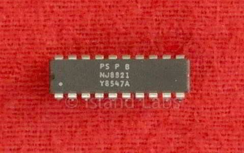
NJ8821 Synthesiser
Features
- Low Power Consumption
- High-Performance Sample and Hold Phase Detector
- Microprocessor Compatible
- >10MHz Input Frequency
- Temperature range = -30°C to +70°C (NJ8821)
- Temperature range = -40°C to +85°C (NJ8821MA)
- Supply voltage = 5V ±0.5V
- Storage temperature -65°C to +150°C
Description
The NJ8821 is a synthesiser circuit fabricated on the GPS CMOS process and is capable of achieving high sideband attenuation and low noise performance. It contains a reference oscillator, 11-bit programmable reference divider, digital and sample-and-hold comparators, 10-bit programmable 'M' counter, 7-bit programmable 'A' counter and the necessary control and latch circuitry for accepting and latching the input data.
Data is presented as eight 4-bit words under external control from a suitable microprocessor.
It is intended to be used in conjunction with a two-modulus prescaler such as the SP8710 series to produce a universal binary coded synthesiser. The NJ8821 is available in Plastic DIL (DP), and Miniature Plastic DIL (MP) packages, both with operating temperature range of -30°C to +70°C. The NJ8821MA is available only in Ceramic DIL package with operating temperature range of -40°C to +85°C.
Programming
When re-programming, a reset to zero is followed by reloading with the new counter values. This means that the synthesiser loop lock-up time is well defined and less than toms. If shorter lock-up times are required when making only small changes in frequency, the GPS NJ8823 (with non-resettable counters) should be considered.
Phase Comparators
The digital phase/frequency detector drives a three-state output, PDB, which provides a 'coarse' error signal to enable fast switching between channels. The PDB output is active until the phase error is within the sample and hold phase detector, PDA, window, when PDB becomes high impedance.
Phase-lock is indicated at this point by a low level on LB. The 'sample and hold' phase detector provides a 'fine' error signal to give further phase adjustment and to hold the loop in lock.
An internally generated ramp, controlled by the digital output from both the reference and main divider chains, is sampled at the reference frequency to give the 'fine' error signal, PDA. When in phase lock, this output would be typically at (VDD-VSS)/2, and any offset from this would be proportional to phase error. The relationship between this offset and the phase error is the phase comparator gain, which is programmable with an external resistor, RB. An internal, 50pF capacitor is used in the sample and hold comparator.
Crystal Oscillator
When using the internal oscillator, the stability may be enhanced at high frequencies by the insertion of a resistor between pin 8 (OSC OUT) and the other components. A value of 150Ω-270Ω is recommended.
Programming/Power UP
Data and signal input pins should not have input applied to them before the application of VDD, as otherwise, latch-up may occur.
