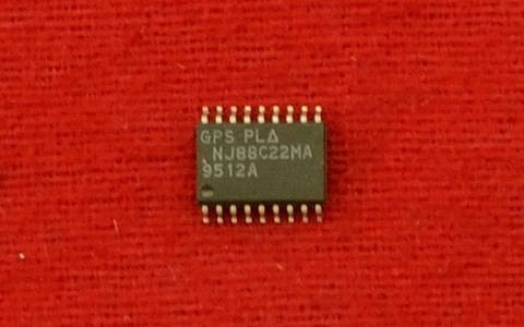
NJ88C22 Synthesiser
Features
- Low Power Consumption
- High-Performance Sample and Hold Phase Detector
- Serial Input with Fast Update Feature
- >20MHz Input Frequency
- Fast Lock-Up Time
- Temperature range = -40°C to +85°C
- Supply voltage = 5V ±0.5V
Description
The NJ88C22 is a synthesiser circuit fabricated on the GPS CMOS process and is capable of achieving high sideband attenuation and low noise performance. It contains a reference oscillator, 11-bit programmable reference divider, digital and sample-and-hold comparators, 10-bit programmable 'M' counter, 7-bit programmable 'A' counter and the necessary control and latch circuitry for accepting and latching the input data.
Data is presented serially under external control from a suitable microprocessor. Although 28 bits of data are initially required to program all counters, subsequent updating can be abbreviated to 17 bits, when only the 'A' and 'M' counters changing. The NJ88C22 is intended to be used in conjunction with a two-modulus prescaler.
Programming
R=fosc/(2 fcomp)
where fosc = oscillator frequency,
fcomp = comparison frequency,
R = 'R' counter ratio.
For example, where the crystal frequency = 10MHz and a channel spacing comparison frequency of 12.5kHz is required,
R=107/(2x12.5x103) = 400
Thus, the 'R' register would be programmed to 400 expressed in binary. The total division ratio would then be 2x400 = 800 since the total division ratio of the 'R' counter plus the ÷2 stage is from 6 to 4094 in steps of 2.
VCO Divider Chain
The synthesised frequency of the voltage controlled oscillator (VCO) depends on the division ratios of the 'M' and 'A' counters, the ratio of the external two-modulus prescaler (P/P+1) and the comparison frequency.
The division ratio N= MP+A, where M is the ratio of the 'M' counter in the range 8 to 1023, and A is the ratio of the 'A' counter in the range 0 to 127.
Note that M>A and
N= fvco /fcomp
For example, if the desired VCO frequency = 275MHz, the comparison frequency is 12.5kHz, and a two-modulus prescaler of ÷64/65 is being used, then:
N = (275x106)/12.5x103 = 22x103
Now, N = MP+A, which can be rearranged as N/P= M+A/P.
In our example we have P = 64, therefore (22x103)/64 =M+ A/64
such that M = 343 and A/64 = 0.75.
Now, M is programmed to the integer part = 343 and A is programmed to the fractional part x 64 i.e. A = 0.75x64 = 48.
To Check: N = 343x64+48 = 22000, which is the required division ratio and is greater than 4032 ( = P2-P).
Phase Comparators
Noise output from a synthesiser loop is related to loop gain:
(KPD KVCO)/N
where KPD is the phase detector constant (volts/rad), KVCO is the VCO constant (rad/sec/volt), and N is the overall loop division ratio. When N is large, and the loop gain is small, noise may be reduced by employing a phase comparator with a high gain.
The sample and hold phase comparator in the NJ88C22 has a high gain and uses a double sampling technique to reduce spurious outputs to a low level.
A standard digital phase/frequency detector driving a three-state output, PDB, provides a ‘coarse’ error signal to enable fast switching between channels.
The PDB output is active until the phase error is within the sample and hold phase detector window when PDB becomes high impedance. Phase-lock is indicated at this point by a low level of LD. The 'sample and hold' phase detector provides a fine error signal to give further phase adjustment and to hold the loop in lock. An internally generated ramp, controlled by the digital output from both the reference and main divider chains, is sampled at the reference frequency to give the 'fine' error signal, PDA. When in phase lock, this output would be typically at (VDD-VSS)/2, and any offset from this would be proportional to phase error. An internally generated ramp, controlled by the digital output from both the reference and main divider chains, is sampled at the reference frequency to give the 'fine' error signal, PDA. When in phase lock, this output would be typically at (VDD-VSS)/2 and any offset from this would be proportional to the phase error.
The relationship between this offset and the phase error is the phase comparator gain, KPDA which is programmable with an external resistor, RB, and a capacitor, CAP. An internal 50pF capacitor is used in the sample and hold comparator.
Crystal Oscillator
When using the internal oscillator, the stability may be enhanced at high frequencies by the inclusion of a resistor between the OSC OUT pin and the other components. A value of between 150Ω and 270Ω is advised, depending on the crystal series resistance.
