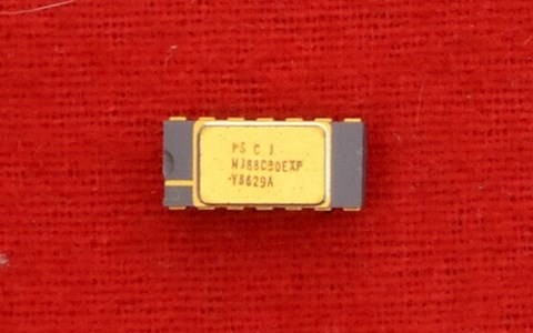
NJ88C30 Synthesiser
Features
- Low Power CMOS
- Easy to Use
- Low Cost
- Single Chip Synthesiser to VHF
- Look Detect Output
- Operating Temperature: -30°C to +85°C
Above an engineering sample marked "EXP" with golden pins and purple ceramic case.
Description
The NJ88C30 contains all the logic needed for a VHF PLL synthesiser and is fabricated on the Plessey high performance, small geometry CMOS process. The circuit includes a reference oscillator and divider, a two-modulus prescaler and 4-bit control register, a 12-bit programmable divider, a phase comparator and the necessary data input and control logic.
Crystal Oscillator and Reference Divider
The Reference oscillator consists of a Pierce-type oscillator intended for use with a parallel resonant fundamental crystal. Typical gain and phase characteristics for the oscillator inverter are shown in Fig 5. An external reference oscillator may be utilised by either capacitively coupling a 1V RMS sinewave into CRYSTAL IN (pin 6) or, if CMOS levels are available, by direct connection to CRYSTAL IN. The reference oscillator drives a 4100 prescaler followed by a reference divider to provide a range of comparison frequencies which are selected by decoding the first three bits (DR2, DR1, DR0) of the input data. The possible division ratios and the comparison frequencies (channel spacing) if a 10MHz crystal is used are shown in Table 1. To assist in trimming the crystal, an open drain output at one hundredth of the reference oscillator frequency is provided on CRYSTAL MONITOR pin 5.
Programmable Divider
The programmable divider consists of a ÷15/16 two modulus prescaler with a 4-bit control register, followed by a 12-bit programmable divider. A 1V RMS sinewave should be capacitively coupled from the VCO to the divider input VCO pin (pin 10). The overall division ratio is selected by a single 16-bit word (DF15 to DF0), loaded through the serial data bus. A lower limit of 240 ensures correct prescaler operation; the upper limit is 65535. The VCO frequency in a locked system will be this division ratio multiplied by the comparison frequency.
Phase Comparator
The phase comparator consists of a digital type phase comparator with open drain f UP and f DN outputs and an open drain LOCK DETECT (LD) output. Open drain outputs from the reference divider and programmable divider are provided for monitoring purposes or use with an external phase comparator. Waveforms for all these outputs are shown in Fig.6. The duty cycle of ‘f UP’ and ‘f DN’ versus phase difference are shown in Fig. 7. The phase comparator is linear over a ±2π range and if the phase gains or slips by more than 2π, the phase comparator outputs repeat with a 2π period. Once the phase difference exceeds 2π, the comparator will gain or slip one cycle and then try to lock on to the new zero phase difference. Note that very narrow pulses may be seen on the inactive phase comparator output at the end of the pulse on the active output.
Data Input and Control Register
To control the synthesiser, a simple three-line serial input is used with DATA, CLOCK and DATA TRANSFER signals. The data consists of 19 bits; the first three, DR2, DR1 and DR0, control the reference divider while the following sixteen, DF15 to DF0, control the prescaler and programmable divider. Until the synthesiser receives the DATA TRANSFER pulse, it will use the previously loaded data; on receiving the pulse it will switch rapidly to the new data.
