SL610 RF Amplifier
RF/IF voltage amplifier with AGC

FEATURES
- 4dB Noise Figure
- High I/P Impedance
- Low O/P Impedance
- 140 MHz Bandwidth (SL610)
- 50dB AGC Range (SL610 - SL611)
- 70dB AGC Range (SL612)
- On-Chip Supply Decoupling
- Low External Component Count
- Operating Temperature: -30°C to +85°C
The SL610C, SL611C and SL612C integrated RF amplifiers are similar circuits, having typical voltage gains of 10, 20 and 50 and upper 3dB gain points at 140MHz, 100MHz and 15MHz respectively. The first two draw a supply current of about 15mA at 6V and have some 50dB AGC range while the SL612C draws 3.5mA and has 70dB of AGC. All three are intended to use with +6V supplies and have internal decoupling. They will drive an output signal of about 1V RMS.
The cross-modulation of the circuits is 40dB down on signal at 1V RMS output with no AGC, and at 250mV RMS input with full AGC. The input and output admittances of the circuits are not significantly affected by AGC level.
Application
There are seven connections to each circuit: input, input bias point, AGC input, the output, the positive supply pin and two earth pins for input and output respectively.
The positive supply should be 6V, but the devices function at supplies of up to 9V. Since internal HF supply decoupling is incorporated, a certain amount of HF ripple can be tolerated in the supply. LF ripple should be kept down as it can cause intermodulation especially at large HF signal levels and 10mV RMS of LF ripple should be considered a maximum.
The AGC characteristic is shown in Fig. 1. It is temperature dependent so that while a potentiometer may be used to provide a gain control voltage the gain so defined is not temperature stable to better than ± 2dB. The AGC terminal typically draws about 200µA at 5V; in some SL610C and SL611C devices, this may be as high as 600µA.
There are two ground connections: pin 4 is the input and pin 8 the output. When several devices are cascaded pin 8 of one stage and pin 4 of the next should have a common ground point; also high common earth impedances to pin 4 and pin 8 of the same device should be avoided.
The input bias point (pin 6) is connected directly to the input (pin 5) and the signal applied through a capacitor but occasionally, when the signal is obtained from a tap on a coil, the arrangement in Fig. 2b may be used to give slightly improved noise performance. CD is a decoupling capacitor. The SL610/611 noise figure is approximately 4 dB at 300Ω source impedance and 6 dB at 50Ω and 2.5kΩ; the noise figure for the SL612 is 3 dB at 800Ω source impedance.
Both the input admittance G11 and the output impedance G22 have negative real parts at certain frequencies. The equivalent circuits of input and output respectively are shown in Figs. 3a and 3b and the values of RIN, ROUT, CIN and LOUT may be determined for any particular frequency from the graphs Figs. 4 and 5. It is seen that for the SL610C and the SL611C, RIN is negative between 30 and 100 MHz, and ROUT is negative over the whole operating frequency range. For the SL612C, RIN is positive, and ROUT is negative only below 700 kHz.
If an inductive element having inductance L1 and parallel resistance R1 is connected to the input, oscillation occurs if RIN is negative at the resonant frequency of CIN and L1 and if R1 is higher than RIN. Similarly, if a capacitor C1 in series with a resistance R2 is connected across the output, oscillation occur if, at the resonant frequency of LOUT and C1, ROUT has a negative resistance greater than the positive resistance R2. Where the input is inductive, therefore, it may be shunted by a 1kΩ resistor; where the load is capacitive, 47Ω should be placed in series with the output.
Suitable input arrangements for the amplifiers are shown in Fig. 2b and Fig. 6. The method shown in Fig. 6a is representative of all inputs; the input and bias points are directly-connected and the signal is coupled via a capacitor. If the input is inductive the 1k resistor shown in Fig. 6b may be required, although usually it can be omitted. If a crystal filter is used it should be correctly terminated, allowing for the impedance of the IC, and coupling made via a capacitor.
The output is a voltage source, with the impedance characteristics mentioned above. Output coupling is via a capacitor, with a series resistor if necessary to preserve stability. If a current output to a tuned circuit is required the arrangement in Fig. 6d is suitable, using almost any small signal NPN transistor with an Ft of over 300M Hz and low COB. To drive particularly low impedances, e.g. a 50 ohm coaxial cable, this impedance should be increased somewhat by a series output resistor (say, 100 ohms) as, if the output is loaded directly by low impedance, most of the negative feedback will be removed with consequently poor linearity and constancy of gain. Examples of the use of these amplifiers are shown in Fig. 7.
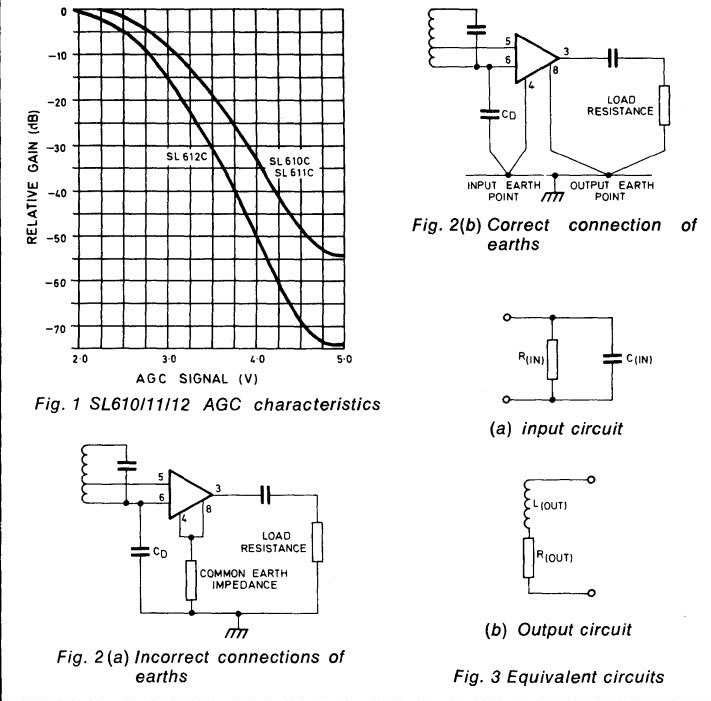
Fig 2
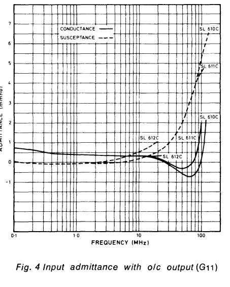
Fig 4
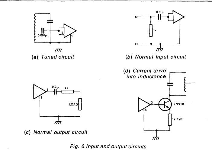
Fig 6

Fig 7
Download and read the article "Simple SSB transceiver" using the SL600 series (Courtesy of Plessey)