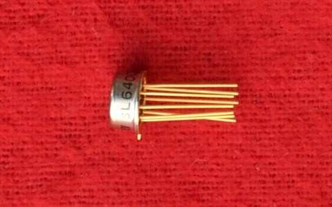
SL640 Balanced Modulator
Features
- No External Bias Networks Needed
- Easy Interfacing
- Choice of Voltage or Current Outputs
- Supply Voltage: 6V
- Conversion Gain: 0dB
Applications
- Mixers in Radio Transceivers
- Phase Comparators
- Modulators
- Maximum Inputs: 200mV RMS
- Ambient temperature: -30°C to +85°C
Description
The SL640C is designed to replace the conventional diode ring modulator, in RF and other communications systems, at frequencies of up to 75MHz. It offers a performance competitive with that of the diode ring while eliminating the associated transformers and heavy carrier drive power requirements.
At 30 MHz, carrier and signal leaks are typically -40dB referred to the desired output product frequency. Intermodulation products are -45dB with a 60 mV rms input signal.
The SL640 has an integral output load resistor (Pin 5) together with an emitter follower output (Pin 6) whereas the SL641 has a single output designed as a current drive to a tuned circuit.
Application Notes
The SL640C and SL641C require input and output coupling capacitors which generally should be chosen to present a low reactance compared with the input and output impedances (see Electrical Characteristics). However, for minimum carrier leak at high frequencies, the signal input should be driven from a low impedance source, in which case the signal input capacitor reactance should be comparable with the source impedance. Pin 2 must be decoupled to earth via a capacitor which presents the lowest possible impedance at both carrier and signal frequencies. The presence of these frequencies at Pin 2 would give rise to poor rejection figures and distortion.
The output of the SL641C is an open collector. If both sidebands are developed across the load, its dynamic impedance must be less than 800 ohms. If only one sideband is significant, this may be raised to 1600 ohms, and it may be further raised if the maximum input swing of 200mV RMS is not used. The DC resistance of the load should not exceed 800 ohms. If the circuit is connected to a +6V supply and the load impedance to +9V, the load may be increased to 1.8kΩ at AC or DC; this, of course, increases the gain of the
circuit.
There are two outputs from the SL640C: one is a voltage source with an impedance of 350 ohms and 8pF, and the other is the emitter of an emitter follower connected to the first output. The output on pin 6 requires a discrete load resistor of not less than 1500 ohms to ground. The emitter follower output should not be used to drive capacitive loads as emitter
followers act as detectors under such circumstances with resultant distortion and harmonic generation. Frequency shaping components may be connected to the voltage output and the shaped signal taken from the emitter follower.
The AC load should not be less than 250Ω.
Signal and carrier leak may be reduced by altering the bias on the carrier and signal input pins, as shown in Fig.4. With the carrier, but no signal, R1 is adjusted for minimum carrier leak.
A similar network is connected to the carrier input, and with signal and carrier present, the signal leak is minimised trimming R2.
