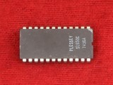
SL650 Modulator
Features
- VFO Frequency Variable Over 100: 1 Range With Same Capacitor: Linearity 0.2%
- Supply sensitivity 20 ppm/% Typ.
- VFO Phase-Continuous at Transitions
- Binary Interface
- Phase-Comparator O/P Can Swing to Supply Voltages
- On-Chip Auxiliary Amplifier (SL650 only)
Applications
- Modems
- Modulators
- Demodulators
- Tone Decoders
- Tracking Filters
- Waveform Generators
Description
The SL650/1 are versatile integrated circuits capable of performing all the common modulation functions (AM, PAM, SCAM, FM, FSK, PSK, PWM, tone-burst, delta-modulation, etc,). A wide variety of phase-locked loops can be realised using the SL650 or SL651, with all parameters accurately controllable; they can also be used to generate precise waveforms at frequencies up to 0.2MHz.
The highly accurate and stable variable frequency oscillator is programmable over a wide range of frequency by voltage, current, resistor or capacitor. In addition direct selection of one of four spot frequencies is facilitated by using the on-chip binary interface, which accepts standard logic levels at very low logic '1' input currents.
The differential input phase comparator has a wide common mode input voltage range. It has a high gain limiting amplifier at its input requiring only lmV input to maintain lock range in a typical phase-locked loop. The current output is programmable from zero to over 2mA by an external resistor or current input, and the gain is voltage -, current -, or resistance -programmable from zero to greater than 10,000.
An auxiliary amplifier with a voltage gain of, typically, 5000 is incorpated in the SL650 for use when it is required to interface to specified levels and impedances. The auxiliary amplifier features low bias current (typically 25nA), fast recovery from overload, and a short-circuit output current of ±7.5mA.
The auxiliary amplifier is omitted from the SL651.
Operating Notes
Basic VFO Relationships
The VFO free-running frequency is inversely proportional to the value of the tuning capacitor C, connected to pins 4 and 5, and directly proportional to the VFO timing current (see Fig.3). Four current switches, controlled by TTL-compatible logic inputs on pins 10 and 11 select a combination of external resistors (connected to pins 6, 7, 8 and 9) which determine the VFO timing current. When both logic inputs are low, open-circuit, or connected to 0V however, then only the current switch associated with pin 7 is closed. the VFO timing current is then determined solely by the value of one resistor (R2 in Fig.3), and by the negative voltage connected to that resistor.
In this simplified configuration, as shown in Fig.4 the VFO frequency is determined by the relationship:
where f is in kHz, V in volts, C in µF and R in kΩ.
It the timing resistor R is returned to the VFO negative supply (pin 3), then
VR = V3
and f = 1/CR
Pin 3 is normally connected to the chip negative supply; if, however, pin 3 is connected to a separate negative supply then the VFO can be voltage-controlled and the VFO frequency will be:
f=1/CR * V-/Vc
where V- is the chip and timing resistor negative supply and Vc is the control voltage connected to pin 3.
The timing current I should be between 20uA and 2mA, corresponding to a value for R between 3kΩ and 300kΩ with supplies of ±6V. For accurate timing, CR should be greater than 5µs.
When the binary interface is used as shown in Fig.3 the VFO free-running frequency is dependent on the logic input states, as shown in Table 1.
