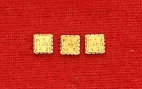
SL6601 FM Receiver
Features
- High Sensitivity: 2µV Typical
- Low Power: 2.3mA Typical at 7V
- Advanced PLL Detector
- Built-in squelch
- Available in Miniature 'Chip Carrier' Package
- 100% Tested for SINAD
The SL6601 is a single or double conversion IF amplifier and detector for FM radio applications. Its minimal power consumption makes it ideal for handheld and remote applications where battery conservation is important. Unlike many FM integrated circuits the SL6601 uses an advanced phase locked loop detector capable of giving superior signal-to-noise ratio with excellent co-channel interference rejection and operates with a second IF frequency up to 1 MHz. Typically the SL6601 will be fed with a first IF signal up to 17 MHz; there is a crystal oscillator and a mixer for conversion to the second IF amplifier, a PLL detector and squelch system. These samples are in small 'Ceramic Chip Carrier' package.
IF Amplifiers and Mixer
The SL6601 can be operated either in a 'straight through' mode with a maximum recommended input frequency of 800kHz or in a single conversion mode with an input frequency of 50MHz maximum and an IF of 100kHz or ten times the peak deviation, whichever is the larger. The crystal oscillator frequency can be equal to either the sum or difference of the two IFs; the exact frequency is not critical. The circuit is designed to use series resonant fundamental crystals between 1 and 17MHz.
If an external oscillator is used the recommended level is 70mV RMS, and the unused pin should be left O/C. The input is AC coupled via a 10nF capacitor.
A capacitor, connected between pin 4 and ground, shunts the mixer output and limit the frequency response of the mixer output and the frequency response of the input signal to the second IF amplifier. A value of 33pF is recommended when the second IF frequency is 100 kHz; 6.8pF is instead for 455 kHz.
Phase Locked Loop
The Phase Locked Loop detector features a voltage controlled oscillator with nominal frequency set by an external capacitor equal to (40 ± 7)/f pF, where f is the VCO frequency in MHz. The nominal frequency may differ from the theoretical, but there is provision for a fine frequency adjustment utilising a variable resistor between the VCO output pins: a value of 470kΩ has negligible effect while 6.8kΩ (recommended minimum value) increases the frequency by approximately 20%. Care should be taken to ensure that the free running VCO frequency is correct; since the VCO and the limiting IF amplifier output produce square waves, it is possible to obtain a lock with the VCO frequency fractionally related to the IF, e.g. IF = 100 kHz, VCO = 150 kHz. This condition can produce good SINAD ratios, but poor squelch performance. The loop filter is connected between pins 11 and 12; a 33kΩ resistor is also required between pin 11 and Vcc. The values of the filter resistor R2 and capacitor C1 must be chosen so that the natural loop frequency and damping factor are suitable for the FM deviation and modulation bandwidth required.
Squelch Facility
When the inputs to the product detector differ in phase a series of current pulses flow out of pin 7. The feature can be used to adjust the VCO; when a 1mV unmodulated input signal is applied to pin 18, the VCO frequency should be trimmed to maximise the voltage on pin 7. The squelch level is adjusted using a preset variable resistor between pin 7 and Vcc to set the output signal to noise ratio at which it is required to mute the output. The capacitor between pin 7 and ground determines the squelch attack time. A value between 10nF and 100nF can be chosen to give the required characteristics. Operation at a signal to noise ratios outside the range 5 - 18 dB is not recommended. Where the front end noise is high (because of very high front end gain), the squelch may well never operate. This effect can be obviated by sensible receiver gain distribution. The load on the squelch output (pin 6) should not be less than 250kΩ; reduction below this level leads to hysteresis problems in the squelch circuit. The use of an external PNP transistor allows hysteresis to be increased. The use of capacitors greater than 1000pF from pin 6 to ground is not recommended.
Outputs
High-speed-data outputs can be taken directly from pins 11 and 12 but normally for audio applications pin 8 is used. A filter network will be needed to restrict the audio bandwidth, and an RC network consisting of 4.7kΩ and 4.7nF may be utilised.
Layout Techniques and Alignment
The SL6601 is not critical in PCB layout requirements except in the 'straight through' mode. In this mode, the input components and circuits should be isolated from the VCO, as otherwise, the VCO will attempt to 'lock' to itself, and the ultimate signal to noise ratio will suffer. The recommended method of VCO adjustment is with a frequency measurement system on pin 9. The impedance must be high, and the VCO frequency is adjusted with no input signal.
Loop Filter Design
The design of loop filters in PLL detectors is a straight forward process. In the case of the SL6601, this part of the circuit is non-critical and in any case will be affected by variations in internal device parameters. The major area of importance is in ensuring that the loop bandwidth is not so small as to allow unlocking with modulation. Damping Factor can be chosen for maximum flatness of frequency response or for minimum noise bandwidth, and values between 0.5 and 0.8 are satisfactory, 0.5 giving minimum noise bandwidth. Design starts with an arbitrary choice of fn, the natural loop frequency. By setting this at slightly higher than the maximum modulation frequency, the noise rejection can be slightly improved. The ratio fm/fn highest modulating frequency to loop frequency can then be evaluated.
