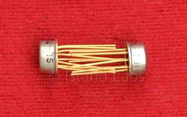
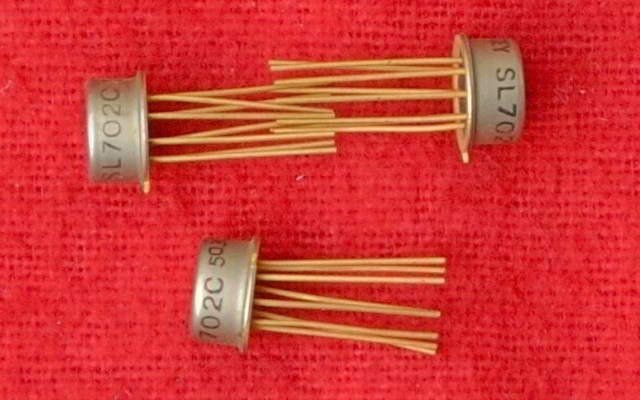
SL701 - 702 DC Amplifier
High Gain Monolithic DC Amplifiers

DESCRIPTION
The SL701B, SL701C, SL702B and SL702C are monolithic, bipolar integrated circuit, high gain DC amplifiers, intended primarily for use as operational amplifiers or in instrumentation applications. The SL701 basic circuit has an internal zener and provides an output symmetrical about earth using the specified supply voltage. The SL702 basic circuit is non-symmetrical, with a direct output, but may be used with an external zener to permit a symmetrical output to with other supply voltages.
The SL701C and SL702C differ from their similar devices with suffix B mainly in having higher maximum input offset voltage.
ABSOLUTE MAXIMUM RATINGS
- Storage temperature range -55°C to +175°C
- Chip operating temperature +175°C
- Supply voltage + 14V and -14V
- Output current 20mA
- Operational Amplifier
- Active Filters
- Instrumentation Applications
- High Gain DC Amplifier
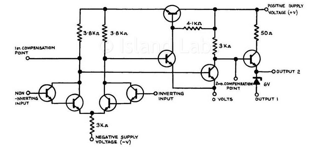
SL701 Internal Diagram
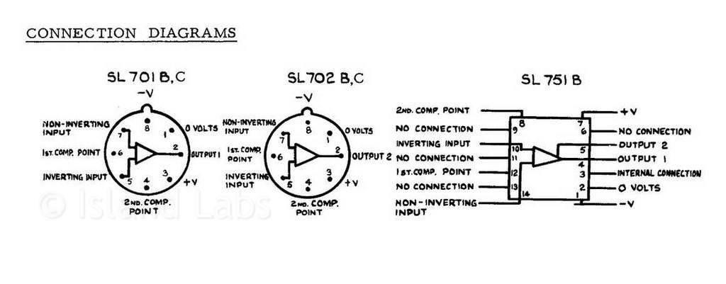
SL701 Connection Diagrams
OPERATING NOTES
Lower Supply Voltages (SL702 — with direct output)
The balance of the collector currents of the input transistors is maintained by an auxiliary internal feedback loop, enabling a range of supply voltages to be used. Since the collector currents of the input transistor are controlled by a 3kΩ 'tail' resistor, the input base current and offset current decrease and the input resistance increase as the negative supply rail voltage is reduced. The open loop gain is also affected by this rail voltage and is virtually proportional to it. A reduction in the positive rail voltage does little except decreases various currents and voltages within the circuit; together with the negative supply, this decreases the maximum available output level. To avoid internal limiting, the magnitude of the positive supply must not be very much lower than that of the negative supply; hence at levels less than the nominal +12 Volts, attention must be paid to the tolerance of the supplies. Typical characteristics for operation under these conditions are given below.
Unity Gain
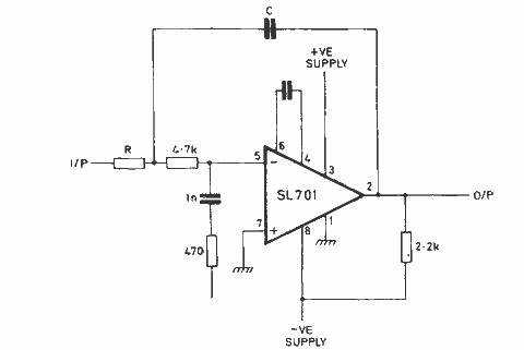
For unity gain more than one method of compensation may be employed; the simplest is shown in Fig. 12. The disadvantages of the technique suggested are that some peculiar overload characteristics may be observed at high frequencies and the maximum signal output without limiting is lower than at higher circuit gains. Circuit K on Fig. 12 gives compensation for a wideband response, allowing approximately 1 dB gain rise above the gain at low frequencies. For maximum signal handling, but reduced noise performance, the method as indicated in Fig. 13 may be used.
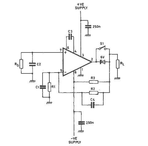
Test Circuit
Part 1. The Device
1.1 GENERAL DESCRIPTION
Amplifiers in this series are general-purpose high-gain DC amplifier units. They are not entirely functional units but are intended for hybrid systems using thin film or conventional components. They then have a wide range of uses. Some which have already been exploited are outlined in part 2 of this article.
The most important section of the amplifier, whose equivalent piece-part circuit is shown in Fig. 1, is the precision comparator "front end". This uses "Darlington" compound pairs in a long-tailed-pair configuration. The balance between the two sides of this comparator is exceptionally well maintained. The transistors are inherently well-balanced being made together in a single chip of silicon. An auxiliary balancing circuit is incorporated in the amplifier which by keeping the standing currents and voltages matched further assists the maintenance of balancing in the comparator. This important circuit feature is described in section 1.2 below.
Following the comparator, there is a common-emitter stage and an emitter-follower output stage. To shift the output voltage level, a 6V zener diode is included in the SL701 version to give a symmetrical swing about the ground with ±12V supplies. The SL702 version is identical except the zener is omitted; this facilitates either an asymmetric output swing or, by choice of external components a balanced swing with lower supply rails. In a flat package having a higher number of leads, both points can be brought out and this version, the SL751, will thus replace either T05 type. The current-handling capacity of the output stage is limited in one direction by the 20mA output current rating and in the other by whatever load resistor is connected to the negative rail. A constant-current tail transistor could be used to improve the negative swing capability. As shown on the circuit diagram, both a collector long-tailed-pair and the common-emitter stage are also brought out. Their prime purpose is to facilitate the use of networks stabilising the feedback loop used with the amplifier. The latter is also useful as an alternative point from which output may be taken.
1.2 THE COMPARATOR BALANCING CIRCUIT
In a simple long-tailed-pair comparator shown in Fig. 2, the "tail" currents defined by the negative supply voltage and the tail resistance, the tail current divides between the two sides. Overall feedback applied to the amplifier has the effect of determining the collector quiescent voltage on the side from which the output is taken. In the SL700 series amplifiers, this voltage is fixed by the input voltage of the following stage. With a fixed positive supply voltage, this will automatically set the collector current in that side of the long-tailed-pair.
Such an arrangement can only remain well balanced with particular values of supply voltages which ensure that the current taken by the opposite side of the long-tailed-pair matches the current fixed on the other side. The circuit is sensitive to changes in the supply voltages or to the effects of a "common mode" or "push-push" signal applied to the two inputs together. Furthermore, dissipations in the comparator's two halves will differ because of the differing collector quiescent voltages. Even with the proper thermal coupling between them, this too will tend to upset the balance.
The auxiliary balancing circuit incorporated in the SL700 series thus makes an essential contribution to the performance. The feedback loop regulates the positive supply voltage to the comparator so that both collector quiescent voltages and currents are substantially the same on each side. Equality of power supply voltages is thus not needed. It is only necessary that the positive supply voltage is not less than say, 3% below the magnitude of the negative supply voltage. It should be noted that the amplifier supply voltage ratings are dependent on several factors, including the load used for the output emitter-follower and ambient temperature. The chart in Fig. 3, therefore, gives the worst-case ratings in graphical form.
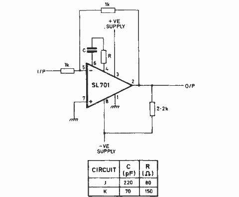
Fig. 12
1.3 Frequency Response And Feedback Stabilization
The typical gain/phase frequency response of the amplifier with guaranteed points is given in Fig.4.
When the external feedback connections are made the resultant loop gain must be cut at a mean rate of less than 9-10dB/octave. A single dominant time constant is often the simplest solution. For example, in the SL701 and similar amplifiers, a capacitor between pins 4 and 6 with a value of a few tens to a few hundred of pF (depending on the feedback fraction ) will give a suitable dominant high frequency cut-off. In general, however, when a particular feedback loop is designed is necessary an appropriate stabilizing network.
Except when maximum bandwidth is required, a dominant lag provided by a 33pF stabilizing capacitor will be found satisfactory for loop gains up to about 20dB short of the full forward gain of the amplifier. (Fig.4 shows gain/phase curves for this configuration also.) The feedback integrator incorporated in the circuits shown in Fig.9 shows how this condition can be satisfied with this important class of circuit. In general, it should be noted that the bandwidth is very wide by conventional circuit standards. Suitable precautions with layout are needed and small supply line decoupling capacitors, say 1000 pF close to the device, are a good choice.