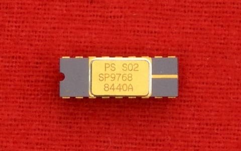
SP9768 DAC
SP9768 8-BIT High-Speed Multiplying D-A Converter
The SP9768 is capable of converting an 8-bit digital signal into an analogue voltage at a rate of over 100 mega samples per second. An inherently low glitch design is used, and the complementary current outputs are suitable for direct transmission line drive. Included on the chip are a precision voltage reference and a reference amplifier. The DAC has current outputs, with a nominal full scale of 20mA, corresponding to a 1V drop across a 50Ω. See Operating Note 2. The actual output current is determined by the on-chip reference voltage and an off-chip current setting resistor. Output current, IOUT, is given by:
IOUT = 4 VREF / VSET at full scale
A complementary IOUT is also provided. The setting resistor, RSET, is typically 220Ω and should have a temperature coefficient similar to that of the output load resistor. Where the load is an oscilloscope, with a 50Ω nominal input, a good quality metal film resistor should be used for RSET. It is important to realise that reflections present in 50Ω load systems will often prove to be a limiting factor in the measurement of settling time. The reference voltage source is nominally 1.280 volts and is of a modified bandgap type, average temperature coefficient of 20ppm/°C from -55°C to +125°C, corresponding to approximately 1 LSB change over this temperature range. To reduce the possibility of instability or noise generation, the reference supply (pin 15) can be decoupled using a high quality ceramic chip capacitor. Stabilisation of the loop amplifier is by a single capacitor from pin 17 to ground. Minimum value is 3900pF, although a 10nF chip ceramic is recommended.
Operating Notes
Measurement of Settling Time
The settling time of the SP9768 is measured for a worst case transition of 0 to full scale. Oscilloscopes, whether real-time or sampling, do not have sufficiently low input VSWR or on-screen resolution for precise settling time measurements (in the 1983). A measurement technique has been designed, shown diagrammatically in Fig.3, in which the DAC can settle into a nearly ideal 50Ω load, with minimal interconnection paths; this is also very closely related to the practical use of the device. Precision settling time measurements can be performed with a high-speed comparator, conveniently a dual device, such as the SP9687, with a minimal delay time, in this case about 2ns. Two references are set up to detect the DAC output settling within a window, conveniently defined as the settling to the ground of the output. The lower comparator detects when the DAC output is coming within ½ LSB of the final settling point, while the upper device checks that there is less than ½ LSB of overshoot.
Output Compliance
Fig.5 shows the method of using the SP9768 with a load resistor not referred to ground. This connection will be used most often when a larger output voltage than that permitted by the -0.7V negative output voltage compliance specification is required. The output resistor can be referred to a positive supply in this case as long as RSET and the analogue ground are also referred to this voltage. If IOUT is also connected to this reference the decoupling will be simplified.
Multiplication Modes
Multiplying operation of the DAC is available in two modes, either a voltage applied in place of the reference, or a current supplied via the current source pin. In the former case the 3dB bandwidth is 250 kHz, while in the latter, operational use exceeds 40MHz.
